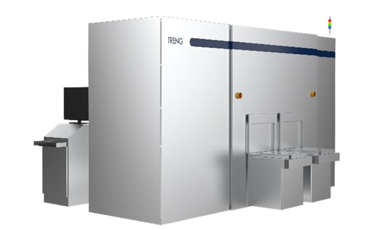
Japanese industrial machinery maker Toray Engineering Co., Ltd. has developed the TRENG-PLP coater, a high-accuracy coating device for panel level packaging (PLP), an advanced semiconductor packaging technology, with a growing demand particularly from AI servers and data centres.
The coater enables 2.5D packaging – a next generation semiconductor production technology – to be applied to larger substrates. Specifically, it is capable of creating detailed rewiring layers on glass substrates for use in interposers, which are a key component of integrated circuits. In this way, the coater facilitates the production of high-performance semiconductors.
Toray Engineering has already delivered pilot TRENG-PLP coaters to a number of major semiconductor manufacturers to demonstrate its capabilities. With sales to commence in December 2024, the company is all set for mass production of the device and is targeting orders totalling 3 billion yen by fiscal 2025, and 6 billion yen by fiscal 2030.
In recent years, increased demand for generative AI servers has resulted in a proliferation of hyperscale data centres. As semiconductor performance has improved, the market for high-performance semiconductors has expanded rapidly; at the same time, this technological progress has driven demand for larger-scale and more efficient advanced semiconductor packaging, which is indispensable for the production of advanced semiconductor devices.
Interposers are a key component in advanced semiconductor packaging, and are traditionally made of silicon. However, since interposers are square and silicon wafers are round in shape, cutting square interposers out of 300mm-diameter round silicon wafers inevitably results in waste silicon. Moreover, as semiconductor performance increases, package sizes have been increasing year on year, leading to fears of further decreases in production efficiency.
PLP technologies, which use 600mm square glass substrates, are seen as a potential solution to the above problems. The larger area of the glass substrate means that larger-scale packages can be produced compared to what is possible with silicon wafers, while its square shape means that the entire substrate can be effectively used to create square interposers without resulting in unused substrate.
Yet the use of PLP technologies to create circuits is not without its own issues: warping of the glass substrate must be prevented, while the wiring materials and photoresist materials must be of a uniform thickness.
To prevent warping, Toray Engineering has developed new technologies for the handling of large glass substrates, drawing on proprietary coating technologies for LCD panels, which are capable of controlling thickness with a high degree of precision. These technologies enable the TRENG-PLP coater to create high-density rewiring layers on 600mm square glass substrates.
Building on Toray’s production technologies for advanced fibre materials, the Tokyo-based company has developed and refined microfabrication technologies for use in semiconductor packaging equipment, display production equipment, and a wide range of other equipment used in the field of electronics. Going forward, Toray Engineering will continue to utilise its high-level production technologies to provide solutions that contribute to society’s forward progress.
